 Kontakt
 Ako nakupovať
Doručenie
Nákupný poradca
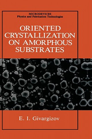
Oriented Crystallization on Amorphous Substrates
 Angličtina
 406 b
406 b
30 dní na vrátenie tovaru
Mohlo by vás tiež zaujímať

 /
/
 Brožovaná
 22.57
€
22.57
€
Present-day scienceand technology have become increasingly based on studies and applications of thin films. This is especiallytrue of solid-state physics, semiconduc tor electronics, integrated optics, computer science, and the like. In these fields, it is necessary to use filmswith an ordered structure, especiallysingle-crystallinefilms, because physical phenomena and effects in such films are most reproducible. Also, active parts of semiconductor and other devices and circuits are created, as a rule, in single-crystal bodies. To date, single-crystallinefilms have been mainly epitaxial (or heteroepitaxial); i.e., they have been grown on a single-crystalline substrate, and principal trends, e.g., in the evolution of integrated circuits (lCs), have been based on continuing reduction in feature size and increase in the number of components per chip. However, as the size decreases into the submicrometer range, technological and physical limitations in integrated electronics become more and more severe. It is generally believed that a feature size of about 0.1um will have a crucial character. In other words, the present two-dimensional ICs are anticipated to reach their limit of minimization in the near future, and it is realized that further increase of packing density and/or functions might depend on three-dimensional integration. To solve the problem, techniques for preparation of single-crystalline films on arbitrary (including amorphous) substrates are essential.


Informácie o knihe
Angličtina
Kategórie

Darujte túto knihu ešte dnes
Je to jednoduché
1 Pridajte knihu do košíka a vyberte možnosť doručiť ako darček 2 Obratom Vám zašleme poukaz 3 Knihu zašleme na adresu obdarovanéhoAhoj! Som Libroamiko, tvoj knižný radca.
Ako ti môžem pomôcť?